Assignment:
A_Redraw the echo hello-world board + Add (at least) a button and LED (with current-limiting resistor.
B_ Check the design rules, and make it.
C_ Group exercise: document how to use a multimeter.
C_ Group exercise: document how to use a multimeter.
A_Redraw the echo hello-world board + Add (at least) a button and LED (with current-limiting resistor.
I started by watching various tutorials from Sparkfun and Jeremy Blum to understand the workflow and better assimilate basic electricity and electronics concepts. And then I Eagle and installed the Fab library and the Adafruit library.
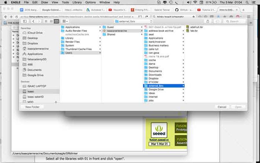
To proceed with the exercise I refered to this basic exercise tutorial that shows explicitly all the steps to get the basic board and to this documentation from Juha Mäkelä of Fablab Oulu from Fab Academy 2016 who uses the copper layer as ground (GND). This is a variation that I feel I can handle.
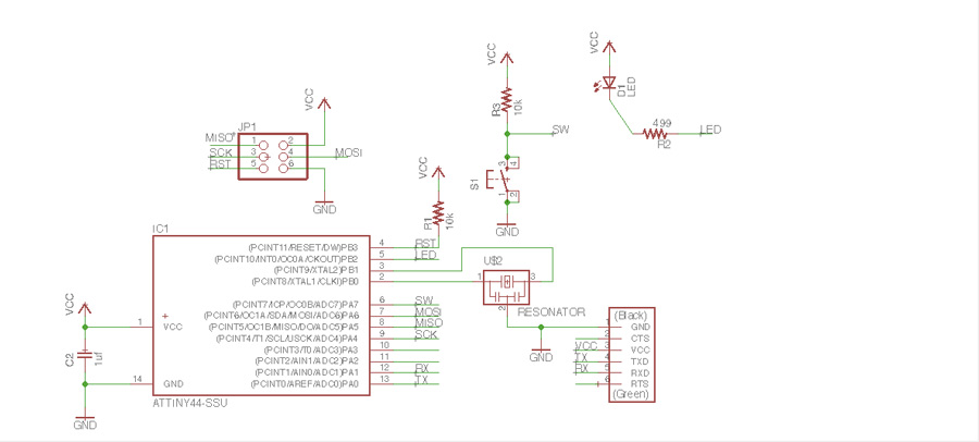
I created a new project, a new schematic and added the components.
- 1 ftdi header: connect the board to the usb port of the computer aloowing datas transmission.
-1 six pin header: to connect the programmer to the board.
-1 attitiny44 microcontroler: the chip of the board and the component where the program will be stored.
-20MHz resonator: this is an external clock which increases the clock speed of the processor of the Attiny and gives it more accuracy.
-10k Resistor: a pull-up resitor which ensure a known state for a signal. It stops unused inputs from floating about randomly when there is no input.
-switch: on/off botton.
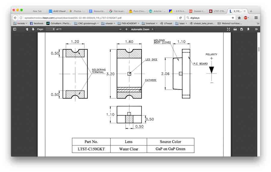
-led (Light emitting diode): When receiving signal it emits light and also serve as a resistor. LEDs have polarity -
-Resistor 499 ohms: its basic use is to reduce current flow, adjust signal levels and divide voltages.
Note: To calculate the resistor's value I applied the Ohm's law - R =V (voltage drop across the LED)/ I (current). Ohm's law and refered to the Smd led datasheet. I will apply a 5v voltage, the datasheet says the component current is 65mA and with a 1.45 v drop voltage. I used this LED RESISTANCE CALCULATOR and got 54.615 ohms. That value is the minimum resistance for this specific components. But the suggested resistor (in the assignment is 499 ohms which I will apply resulting only in dimming the SMD led brightness.
Apart from these components in the schematic I added the VCC and the GND which are not components but essential elements in the board design.
I found confusing that the representation of the Attiny in the schematic be so different to the actual component so I kept them both at hand as I constantly had to refer to them to connect the pins.

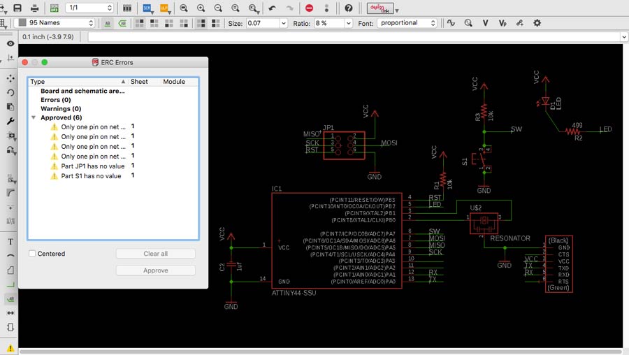
I ran into trouble trying to connect the elements in the schematics and struggled to find what the reason was. Eventually I realized that I had labeled the components using the "text" command instead of the "label/name" command making impossible for Eagle to link the elements. After relabeling all the components evertyhting connected except for the ground connections. I went back to the library and changed the ground symbol I had used to another one and that made it work. I ran aother ERC (schematic desigtn rule) and had some errors that persisted. After analysing and consulting with my instructor I concluded thoses errors coincide with microcontroler pins that are not connected and 2 components that have no values assigned to them. Which are the switch and the 6 pin headers. That will not affect the design so I decided to approve the design rules and move on.
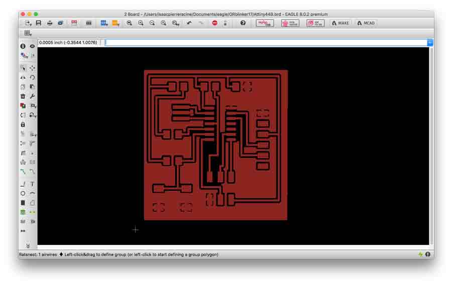
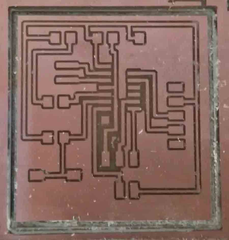
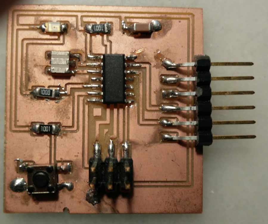
Tracing the board was a lot of work but I enjoyed it as it was more concrete - can see the board represented grafically. I did redistributed the components on the board in comparison to the template board but did not add any new components. I wanted to keep time to really get familiar with the different aspect of the application. Once I got it right I connected the ground to the copper layer of the board. I created a rectangle outside the board limit (white frame)using the polygone command (in the bottom section of the vertical tool bar) , naming the rectangle as ground (GND) - this converts the rectangle lines in dots.
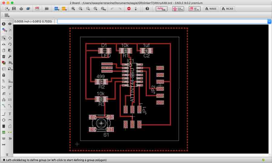
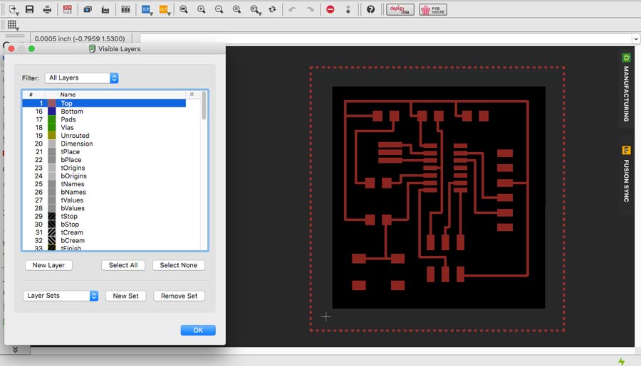
I deselect all the layers except for the Top (first icon on the top of the vertical toolbar). Only the traces remain apparent on the board. This could be done after but all the graphics of the components and labelling really distracted me.
B_Check the design rules, and make it.
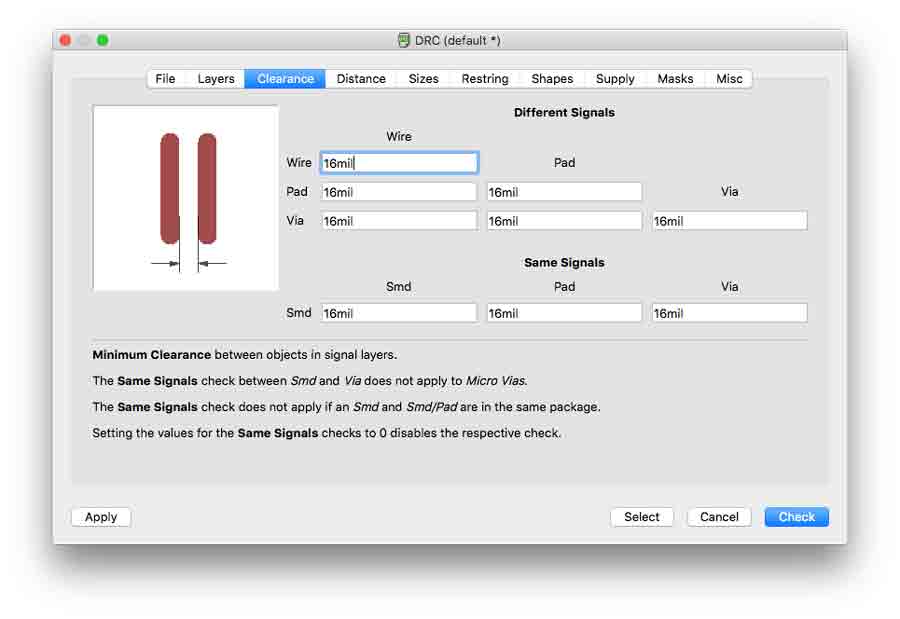
Before completing the conversion of the base layer into ground I ran the design rules (DRC in the top menu/tools).The tutorials recommended to set clearance at 12mils (1/1000inch) but I will be milling with a 1/64th inch bit which corresponds to 16mils - it will only make the trace wider which is even better.
I received 6 clearance errors and 3 air wire error.
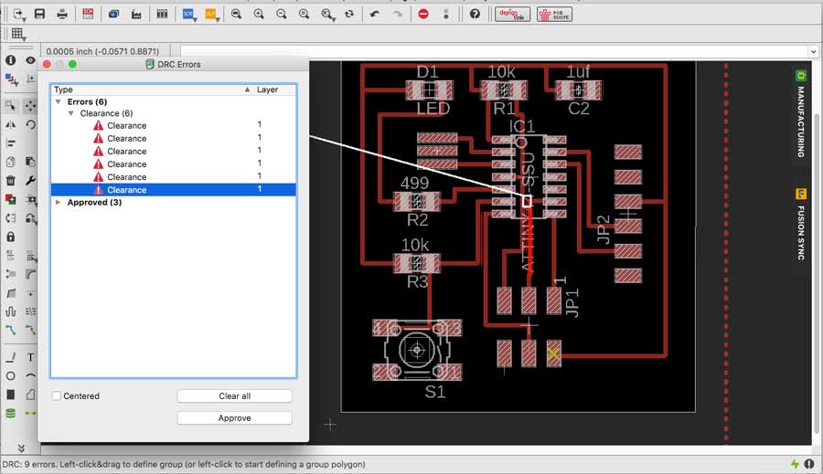
I easily fixed the clearance error by moving slightly the trace away from the other traces that was giving the conflict but I could not get to fix the air wire error. I figured it may be related to the component specifications and decided to approve and move on. I do not see how it can affect the functioning of the board as they are related to pins that will be connected to ground, and the ground will be the copper layer. If well soldered there is no way that it would cause a problem.
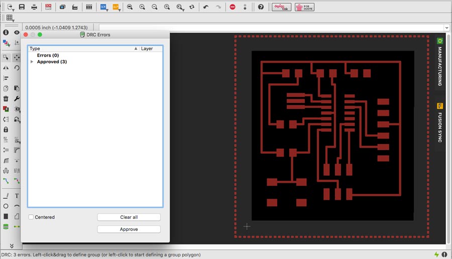
Finally I converted the base layer into a ground by clicking the "rastnest" - the background of the board turns to red.
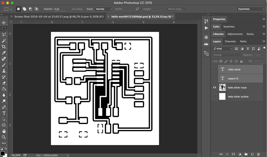
The file needs to be exported from Eagle to PNG (file menu/export/image). It is a pretty simple process but it has some little tricks -making shure the monochrome option is clicked on so the image is converted to black and white, put resolution to at least 1000dpi (up to 1500).
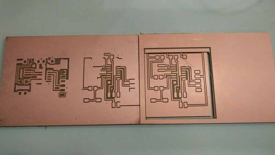
I did this process using photophop: I opened thre PNG in Photoshop. It opens as an index file and needs to be converted into a grey scale image so it can be edited (image7mode/greycscale). From the same png file we create the trace and the outline. The trace is as is and the outline is made by creating a white layer frame that is 32mil (2 x width of the traces) wider than the frame of the trace frame. The editing of the image consists in creating 2 separete files: one for the trace and another one for the outline. Each layer has to be exported as individual PNG files.
Milling the board is usual business: open the file in the fab module, set the parameters on the module, prepare the copper board on the Modela bed and set the axes (X/Y and Z). The firt intent did not come out well as I did not realized I had to invert the image when milling a board designed with the copper layer as GND. I repeated a 2nd time but it neither came out well because the board was too small and part of the milling area was out of the board. I repeated it and again it failed. For some reason (could not find a logical reason except that I must have made a mistake and choose the wrong file when loading it to the fabmodule) so the outline file did not lined up properly with the trace file therefore cutting the traces on one side of the board.
Before going on milling another board I tried tinkering my failed board using cable to bridge the traces that had not been milled properly. I spend quite a bit of time but I could not make it to work properly. I liked the idea to make a board that was everything but orthodox so I persevered in trying. I got a green light from AVR programmer when connecting it to my board but nver got to bootload it.
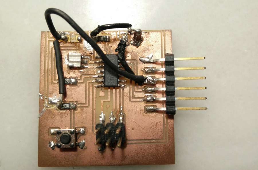
I identified some short-circuits and tried to resoldered but it became really messy so I surrendered and decided to mill a new one. This time I did the milling at Green Fablab and there were no double-face tape so I had to invent a way to hold the board to the machine bed. While doing the tracing it moved a little bit but did not make any dammage.
I had a little struggle with the led. I did not get any error message but could not get the led to lit. It was connected the wrong way. There is a a tiny green stripe on the cathode (-)pole that has to be connected to GND and the anode (no stripe) to VCC.
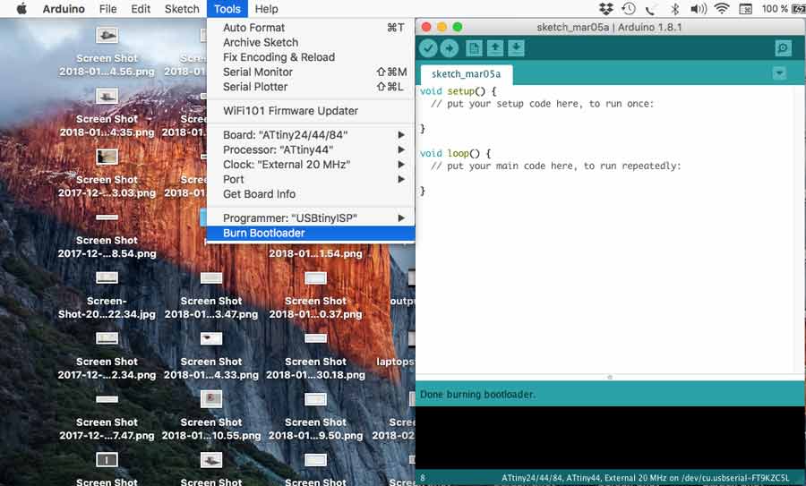
I connected the board with the FTDI cable to one of the USB port of my computer and on the other I connected my FABISP. And I connected the 6 pin headers of the FabISP and the Hello board.
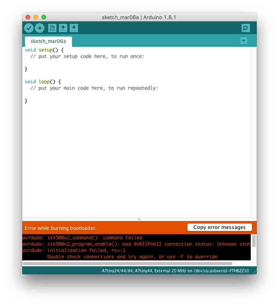
I opened Arduino ID (which I had installed already) configured it for the FabISP to program the Hello Board. The parameters to set up are:
-Board: ATtiny24/44/84
-Processor: ATtiny44 (microcontroller of the Hello Board)
-Clock: 20MHz external (resonator on the Hello Board - exterior means it is not integrated in the microcontroler)
-Port: serial port - when FTDI cable is connected to USB port it shows in the post option in the menu (serial port option).
-Programmer: USBtinyISP (because I use my FabISP)
Once it is all configured click on BOOTLOADER and the application will bootload the Hello Board. That means it makes it ready to receive a program.
The board is tested and ready to be programmed for the next electronic assignment. This week helped me get more familiar and comfortable with the electronic design workflow (schematic and board), the components, milling and soldering. I feel very satisfied with the experience.
C_ Group exercise: document how to use a multimeter.
As in many other occasion my group is composed of my-self only since I am formally not part of this year's alumni program, thus not assiting to class on a constant basis. Neverhtless I am sharing this documentation with my fellow student in case anyone can benefit from it.
The Multimeter tutorial from Sparkfun explains very well what is a Multimeter, why, when and how to use to use its main functions. This How to use a multimeter from wikihow web site is also a helpful read just as well as the Wikipedia multimeter page. My documentation resume my beginner understanding of the multimeter instrument.
A
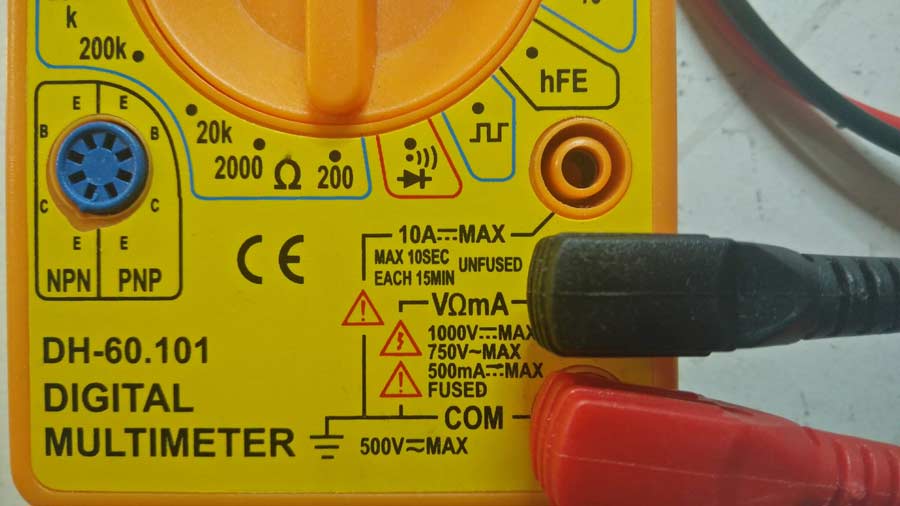
The multimeter has 3 main parts:
-Display
-selectioni knobs
-Ports (+ probes)
The display indicates the reading of values selected with the selection knob - such as:
-voltage (volts_V)
-current (milliamps_mA)
-resistance (ohms_Ω)
Like most multimeter mine is not autoranging which means it needs to be set to a range it can measure. For example 2V measures up to 2Volts and 20V up to 20Volts, So if you’ve measuring a 12V battery, use the 20V setting, and like this for each different values. That explains the different positions of the selection knob.
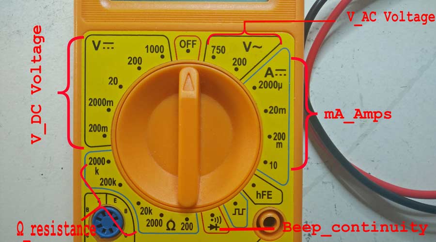
There are 3 ports but the probes can only be connected to 2 ports at a time. Conventionally the black probe connects to the COM (for common) port and to the GND or "-" of the circuit. The red probe can be connected to either of the two ports left depending on the level of current to be measured. Most often we use the VΩmA port which has a fuse and allows reading of up to 500mA, 750V AC and 1000V DC. The other port is considered the special port and serves for values up to 10Aamps . It is considered a special one because we mostly use multimeter to measure low voltage and Amps in electronic circuitry. In case of measuring higher voltage special consideration have to be taken that I will not cover in this documentation.
Note: Switching probes will not damage the multimeter but a positive value will become a symetrically negative value.
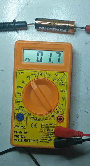
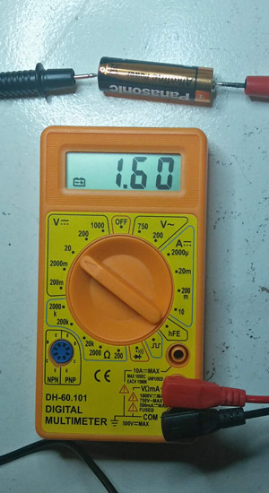
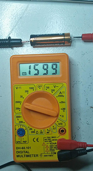
To measure the Dc Voltage ( on the mutlimeter DC Voltage range has a V with a straight line next to it) set the selection knob to a range higher than the circuit estimate voltage. Press the black probe to GND and red probe to V of the circuit or battery. If selected voltage is too low Multimeter will display a 1 indicating sturation.
In the following sequence it shows very obvious how selecting the closst position to the max voltage measured gives a more accurate reading. I am measuring a 1.5v battery. The batery is out of the box so it gives slightly more than 1.5V:
-When I set it to 200V it reads 1.7V
- when I set it to 20V it reads 1.60V
- when I set it to 200mV it reads 1599 millivolts.
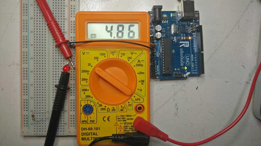
Continuing with reading voltage I read the voltage of a 5V Arduino input through a led.
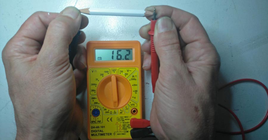
To measure the resistance. Connect each probe to each end of the resitor. Reading will be the resistance of the materials measured. I used a graphite pencil. I could have very well connect the probes to respectiv end pin of any resistor and would have collect theresistor's value. Resitors have 5% tolerance, sometime up to 10% which may cause variations as to its equivalent in the value based on the color code of the reistors
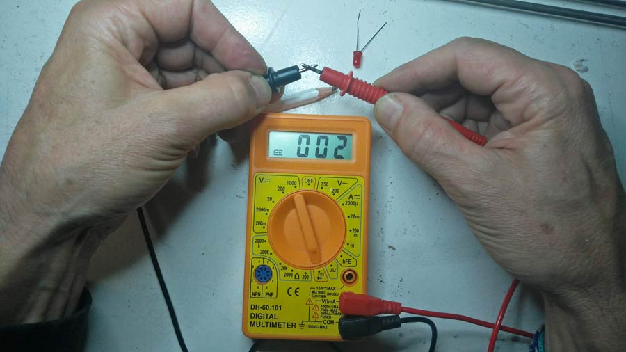
To test the continuity. Pressing the two probes together with the selection knob on the continuity position will emit a sound. When the probes are in contact with 2 pins or ports that should be connected the multimeter will beep indicating th ecurrent goes through. If it does not beep there is a connection or design problem. This functions is widely use to diagnose circuit relvance.
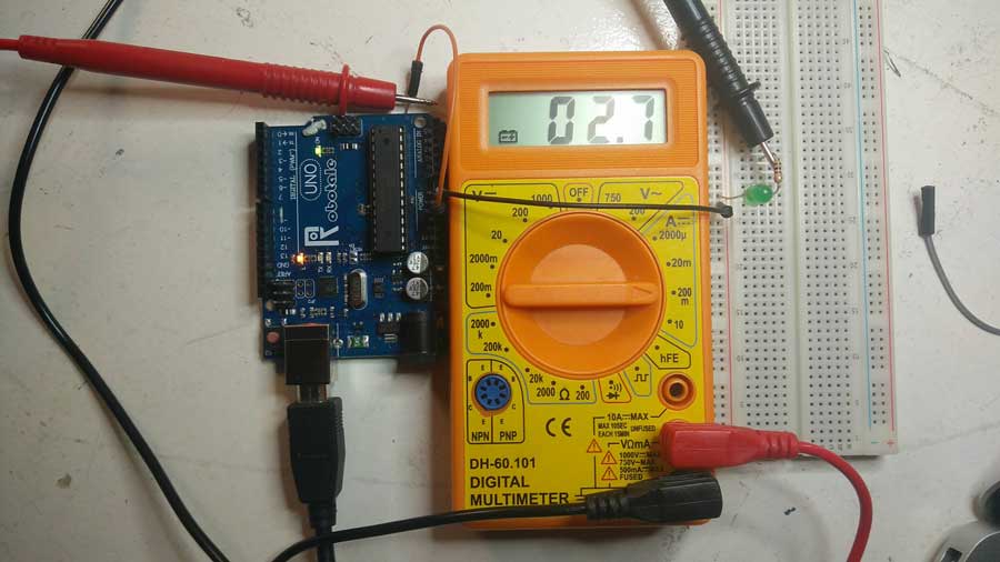
Reading current is one of the trickiest and most insightful readings in the world of embedded electronics. It’s tricky because you have to measure current in series. Where voltage is measure by poking at VCC and GND (in parallel), to measure current you have to physically interrupt the flow of current and put the meter in-line.
I have connected the GND ('-') arduiono to the cathode of Led and to the resistor. I have conected the black probe to the GND of coming from the Ardiuino and the red to the 5V of the Arduino. The current od the circuit is 2.7mA.
Researching on electrcity to document the multimeter i gathererd a series of links and tutorals showing there is more to it in electricity than what the basic function of a multimeter can read. Nevertheless theese 4 main functions of the multimeter are the most used for what we are doing so far in our assignments. Further issues such as freuency will be covered in the "network and communicaton" assignment when I will document the oscilloscope. Here some interesting references.
Frequency measurement.
the "μ" symbol.
Electric units rapid table
Conclusion
I had to get used to the new application (Eagle) and get into completely new territories. Many of what I did at the beginninmg did not make any sense as I could not assimilate everything at once but surprisingly I grasp fairly quickly the workflow in Eagle - the schematic /vs/ the board, selecting the component, tracing, ect. Nevertheless I cannot yet imagine how I could design a board from scratch. I did not prentend to be creative in any ways with this exercise but limit my-self to acquire the technical skills and get better at the work flow involved in the process. The combination of the 2 tutorials I followed were very helpful to get me through and feel satisfied with all I learned.